Find HDI PCB Market, HDI PCB Cost, HDI PCB Price on Industry Directory, Reliable Manufacturer/Supplier/Factory from China.
| Payment Type: | L/C,T/T,D/P,Paypal,Money Gram,Western Union |
|---|---|
| Incoterm: | FOB,CFR,CIF,EXW,FCA,CPT,CIP |
| Min. Order: | 1 Piece/Pieces |
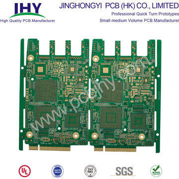
HDI Technology PCB Prototype
HDI PCB (High Density Interconnector PCB), HDI Technology PCB is a circuit board having a relatively high line distribution density using the micro-blind and buried hole technology.
It is a process that includes an inner layer line and an outer layer line, then uses a hole and a metallization in the hole to realize a joint function between the inner layers of each layer.
With the development of high-density, high-precision electronic products, the same requirements are imposed on circuit boards. The most effective way to increase the density of pcb is to reduce the number of through holes, and to accurately set the blind holes and buried holes to achieve this requirement, thereby generating an HDI Technology PCB.
We offer low-volume, Prototype and Production PCB fabrication service, for HDI PCB, rigid PCB, flexible PCB, High Tg boards, etc. All project comes with satisfaction guarantee and on-time delivery.
The attributes of the displayed product
Type HDI PCB Layers 8 Layer Base Material FR4 Tg170 Dielectric Prepreg Board Thickness 1.6mm±10% Copper Weight 1oz Surface Finish ENIG 2U"+Gold Plating 30U" Minimum trace Width/Spacing 0.1/0.1mm(4/4mils) Solder Mask Color Green Silkscreen Color White Min. Hole Size 0.15mm Via in Pad Yes Epoxy Via Plug Yes Hole Copper Wall Thickness 25.4um Controlled Impedance Yes Flame Retardant Properties 94 V-0 Application Industrial Controllers
The Concept
HDI: High Density Interconnection Technology. It is a multilayer board made by a build-up method and a micro-blind buried hole.
Micro-hole: In a PCB, a hole less than 6 mil (150 um) in diameter is called a micro-hole.
Buried Via: buried in the inner layer of the hole, not visible in the finished product, mainly used for the conduction of the inner layer line, can reduce the probability of signal interference, and keep the continuity of the characteristic impedance of the transmission line. Since the buried via does not occupy the surface area of the PCB, more components can be placed on the surface of the PCB.
Blind Via: connecting the surface layer and the inner layer without passing through the full-board via holes.
Key HDI PCB Benefits
The evolution of high-density PCB technology has given engineers greater design freedom and flexibility than ever before. Designers using HDI high density interconnect methods now can place more components on both sides of the raw PCB if desired. In essence, an HDI PCB gives designers more space to work with, while allowing them to place smaller components even closer together. This means that a high-density interconnect PCB ultimately results in faster signal transmission along with enhanced signal quality.
HDI PCB is widely used to reduce the weight and overall dimensions of products, as well as to enhance the electrical performance of the device. The high-density PCB is regularly found in mobile phones, touch-screen devices, laptop computers, digital cameras and 4G network communications. The HDI PCB is also prominently featured in medical devices, as well as various electronic aircraft parts and components. The possibilities for high-density interconnect PCB technology seem almost limitless.
HDI Printed Circuit Boards Structures:
Application: Cell phone, UMPC, MP3 Player, PMP, GPS, Memory Card

Application: Cell phone, PDA, UMPC, Portable game console, DSC, Camcorder
2+N+2 HDI PCB Structure:

Application: Cell phone, UMPC, MP3, PMP, GPS, Memory card.

Product Categories : HDI PCB